- 您现在的位置:买卖IC网 > Sheet目录3841 > PIC18F67K22-I/PTRSL (Microchip Technology)MCU PIC 128K FLASH XLP 64TQFP
2009-2011 Microchip Technology Inc.
DS39960D-page 13
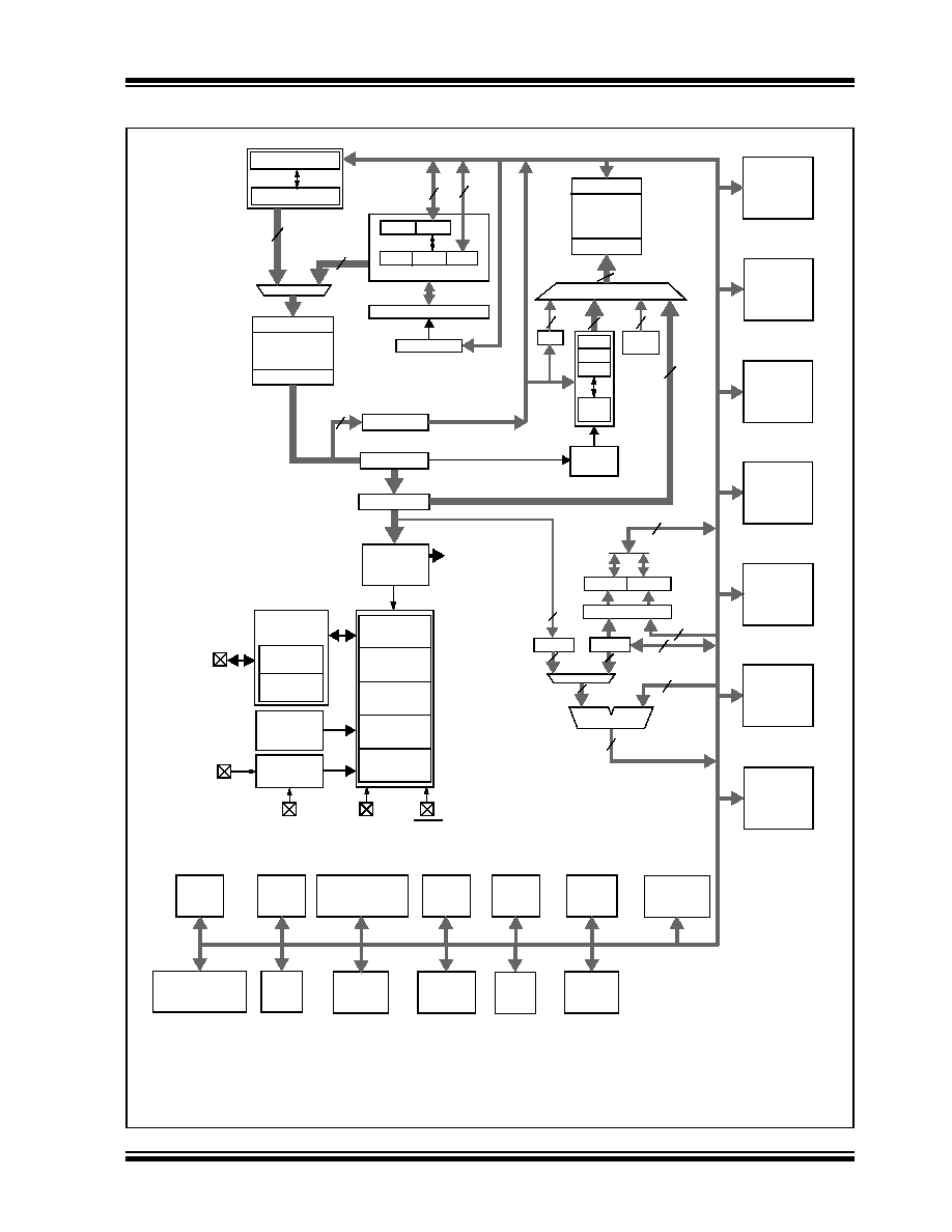
PIC18F87K22 FAMILY
FIGURE 1-1:
PIC18F6XK22 (64-PIN) BLOCK DIAGRAM
Instruction
Decode and
Control
PORTA
Data Latch
Data Memory
(2/4 Kbytes)
Address Latch
Data Address<12>
12
Access
BSR
FSR0
FSR1
FSR2
inc/dec
logic
Address
4
12
4
PCH
PCL
PCLATH
8
31-Level Stack
Program Counter
PRODL
PRODH
8 x 8 Multiply
8
BITOP
8
ALU<8>
Address Latch
Program Memory
Data Latch
20
8
Table Pointer<21>
inc/dec logic
21
8
Data Bus<8>
Table Latch
8
IR
12
3
PCLATU
PCU
Note
1:
See Table 1-3 for I/O port pin descriptions.
2:
RA6 and RA7 are only available as digital I/O in select oscillator modes. For more information, see Section 3.0 “Oscillator
.
3:
Unimplemented on the PIC18F65K22.
EUSART1
Comparator
MSSP1/2
3/5/7(3)
2/4/6/8/10(3)/12(3)
CTMU
Timer1
ADC
12-Bit
W
Instruction Bus <16>
STKPTR
Bank
8
State Machine
Control Signals
Decode
8
EUSART2
ROM Latch
PORTC
PORTD
PORTE
PORTF
PORTG
RA0:RA7(1,2)
RC0:RC7(1)
RD0:RD7(1)
RE0: RE7(1)
RF1:RF7(1)
RG0:RG5(1)
PORTB
RB0:RB7(1)
OSC1/CLKI
OSC2/CLKO
VDD,
Timing
Generation
VSS
MCLR
Power-up
Timer
Oscillator
Start-up Timer
Power-on
Reset
Watchdog
Timer
BOR and
LVD
Precision
Reference
Band Gap
INTRC
Oscillator
Regulator
Voltage
VDDCORE/VCAP
ENVREG
16 MHz
Oscillator
Timer0
4/5/6/7/8/9(3)/10(3)
RTCC
Timer
1/2/3
CCP
ECCP
1/2/3
发布紧急采购,3分钟左右您将得到回复。
相关PDF资料
PIC18F66K90-I/MRRSL
MCU PIC 64K FLASH MEM XLP 64QFN
PIC16LC621-04/SO
IC MCU OTP 1KX14 COMP 18SOIC
PIC18LF2410-I/SP
IC MCU FLASH 8KX16 28-DIP
DSPIC30F3013-20I/SP
IC DSPIC MCU/DSP 24K 28DIP
PIC18LF6390-I/PT
IC PIC MCU FLASH 4KX16 64TQFP
DSPIC30F3013-30I/SP
IC DSPIC MCU/DSP 24K 28DIP
DSPIC33FJ32MC202-E/SO
IC DSPIC MCU/DSP 32K 28SOIC
52745-0896
CONN FFC 8POS .5MM R/A ZIF SMD
相关代理商/技术参数
PIC18F67K22-I/PTRSL
制造商:Microchip Technology Inc 功能描述:IC 8BIT MCU PIC18F 16MIPS 制造商:Microchip Technology Inc 功能描述:IC, 8BIT MCU, PIC18F, 16MIPS, TQFP-64
PIC18F67K22T-I/MR
功能描述:8位微控制器 -MCU 128kB Flash 4kB RAM
RoHS:否 制造商:Silicon Labs 核心:8051 处理器系列:C8051F39x 数据总线宽度:8 bit 最大时钟频率:50 MHz 程序存储器大小:16 KB 数据 RAM 大小:1 KB 片上 ADC:Yes 工作电源电压:1.8 V to 3.6 V 工作温度范围:- 40 C to + 105 C 封装 / 箱体:QFN-20 安装风格:SMD/SMT
PIC18F67K22T-I/MRRSL
功能描述:8位微控制器 -MCU 128KB Flash 4KB RAM nanoWatt XLP GP RoHS:否 制造商:Silicon Labs 核心:8051 处理器系列:C8051F39x 数据总线宽度:8 bit 最大时钟频率:50 MHz 程序存储器大小:16 KB 数据 RAM 大小:1 KB 片上 ADC:Yes 工作电源电压:1.8 V to 3.6 V 工作温度范围:- 40 C to + 105 C 封装 / 箱体:QFN-20 安装风格:SMD/SMT
PIC18F67K22T-I/PT
功能描述:8位微控制器 -MCU 128kB Flash 4kB RAM
RoHS:否 制造商:Silicon Labs 核心:8051 处理器系列:C8051F39x 数据总线宽度:8 bit 最大时钟频率:50 MHz 程序存储器大小:16 KB 数据 RAM 大小:1 KB 片上 ADC:Yes 工作电源电压:1.8 V to 3.6 V 工作温度范围:- 40 C to + 105 C 封装 / 箱体:QFN-20 安装风格:SMD/SMT
PIC18F67K22T-I/PTRSL
功能描述:8位微控制器 -MCU 128KB Flash 4KB RAM nanoWatt XLP GP RoHS:否 制造商:Silicon Labs 核心:8051 处理器系列:C8051F39x 数据总线宽度:8 bit 最大时钟频率:50 MHz 程序存储器大小:16 KB 数据 RAM 大小:1 KB 片上 ADC:Yes 工作电源电压:1.8 V to 3.6 V 工作温度范围:- 40 C to + 105 C 封装 / 箱体:QFN-20 安装风格:SMD/SMT
PIC18F67K90-E/MR
功能描述:8位微控制器 -MCU 128KB Flash 4KB RAM LCD
RoHS:否 制造商:Silicon Labs 核心:8051 处理器系列:C8051F39x 数据总线宽度:8 bit 最大时钟频率:50 MHz 程序存储器大小:16 KB 数据 RAM 大小:1 KB 片上 ADC:Yes 工作电源电压:1.8 V to 3.6 V 工作温度范围:- 40 C to + 105 C 封装 / 箱体:QFN-20 安装风格:SMD/SMT
PIC18F67K90-E/PT
功能描述:8位微控制器 -MCU 128KB Flash 4KB RAM LCD
RoHS:否 制造商:Silicon Labs 核心:8051 处理器系列:C8051F39x 数据总线宽度:8 bit 最大时钟频率:50 MHz 程序存储器大小:16 KB 数据 RAM 大小:1 KB 片上 ADC:Yes 工作电源电压:1.8 V to 3.6 V 工作温度范围:- 40 C to + 105 C 封装 / 箱体:QFN-20 安装风格:SMD/SMT
PIC18F67K90-I/MR
功能描述:8位微控制器 -MCU 128kB Flash 4kB RAM LCD
RoHS:否 制造商:Silicon Labs 核心:8051 处理器系列:C8051F39x 数据总线宽度:8 bit 最大时钟频率:50 MHz 程序存储器大小:16 KB 数据 RAM 大小:1 KB 片上 ADC:Yes 工作电源电压:1.8 V to 3.6 V 工作温度范围:- 40 C to + 105 C 封装 / 箱体:QFN-20 安装风格:SMD/SMT